— CAPABILITIES
HDI PCB Capability
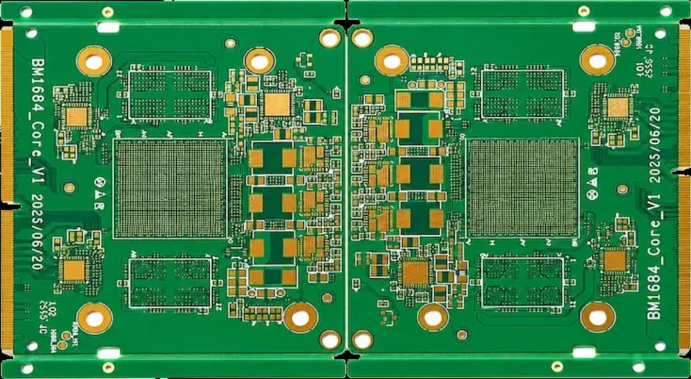
HyperPCB builds high-density interconnect PCBs from 1+N+1 to 4+N+4 and ELIC, with laser microvias down to 50 µm, 0.10 mm mechanical drills and 1:1 blind via aspect ratio — up to 48 layers with ±7% controlled impedance.
— SPECIFICATIONS
Capability & tolerance chart
| Parameter | Standard | Advanced |
|---|---|---|
| HDI Structures | 1+N+1, 2+N+2, 3+N+3, 4+N+4, ELIC | Any-layer HDI by project review |
| Maximum Layer Count | Up to 48 layers | — |
| Minimum Line Width / Spacing | 1.57/1.57 mil | 1.38/1.38 mil for advanced high-density products |
| Minimum Mechanical Drill | 3.94 mil | — |
| Minimum Laser Via | 2.76 – 2.95 mil standard HDI | 1.97 mil for advanced HDI |
| Minimum Laser Via Pad | 8.86 mil | Smaller pads by project review |
| Through-Hole Aspect Ratio | Up to 16:1 | — |
| Blind Via Aspect Ratio | Up to 1:1 | — |
| BGA Pitch | Down to 11.8 mil, subject to design and process review | — |
| Via Filling | Copper-filled, resin-filled, filled and capped vias | — |
| Via Structures | Stacked, staggered, blind, buried and via-in-pad | — |
| Controlled Impedance | ±8% typical | Tighter control by stack-up review |
| Copper Thickness | 1/3 oz – 8 oz, depending on layer structure | — |
| Lamination Cycles | Multiple sequential lamination cycles supported | — |
| Surface Finishes | ENIG, ENEPIG, OSP, immersion silver, immersion tin, hard gold, soft gold, gold finger | — |
Sequential lamination without registration surprises
Every HDI build adds lamination cycles, and each cycle is an opportunity for layer-to-layer drift. We image with LDI, drill microvias by laser on the same panel reference, and measure registration between cycles rather than at final inspection, so a 4+N+4 build lands inside the same pad windows as a 1+N+1.
Choosing a structure for your BGA pitch
A 0.5 mm pitch BGA usually escapes on 1+N+1. Below 0.4 mm, or with several fine-pitch devices sharing a region, 2+N+2 and stacked or staggered microvias start to pay for themselves. Send the densest footprint on the board and we will come back with the cheapest structure that routes it.
Verification on buried structures
Buried microvias cannot be inspected optically once laminated, so coupons are cross-sectioned and 3D X-ray is used on the finished board to confirm fill, wetting and stack alignment. Records ship with the lot.
— FAQ
Frequently asked questions
— RELATED
Related capabilities
Ready to build?
Upload your Gerber files for a free DFM review and a quote within 24 hours. Mutual NDA available.